
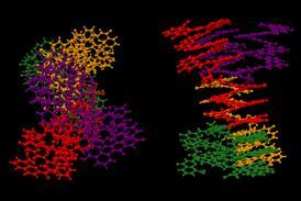


Helicene columns could confer chiral properties on optoelectronic devices
Organic and inorganic templates control the crystallisation of helicenes in bulk, providing a simple and effective way to integrate chirality into optics and electronics
Controlling the chirality of organic semiconductors could enhance their efficiency and bring new functionalities to devices. However, manufacturing materials with tuneable chirality in bulk has remained a challenge – so far only a few examples of oriented monolayers had been reported. Now, a multidisciplinary team of researchers in the UK, Canada and Japan has developed a simple templating method to grow ordered chiral thin films for a wide range of applications.
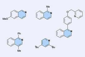
‘Thanks to computational design and clever synthesis we knew we had really exciting materials,’ says lead author Jess Wade from Imperial College London, UK. ‘Organic semiconductors already showcase interesting properties, they’re lightweight, low-cost, biocompatible and highly tuneable.’ Adding chirality to the list could enhance the existing properties of optoelectronics, used in displays, sensors, solar panels, transistors and more. ‘Moreover, with chirality, we can manipulate the spin of photons and electrons at room temperature,’ she says. ‘But to do that in devices, we needed to control chiral properties in the bulk.’